
Goals
The goal of this lab was to do Sputtering and ALD which are two processes commonly used to deposit materials on Silicone wafers. We started with 4 inch <100> wafers and compaired the deposition with both processes.
Sputtering
Sputtering is what we call a physical vapor deposition (PVD) technique that is used to deposit thin films of material on a silicone wafer. The advantages of this technique is the speed with it being able to deposit at a rate of 1 Angstrom per second.
Our process
Our ultimate goal is to get a layer of Platinum on the silicone wafer. That being said, we need somthing called an adhesion layer as we cannot deposit Platinum directly on the Silicone wafer. Since we are doing what is called a Heteroepitaxy process (depositing different materials) we need to ensure the two materials stick.
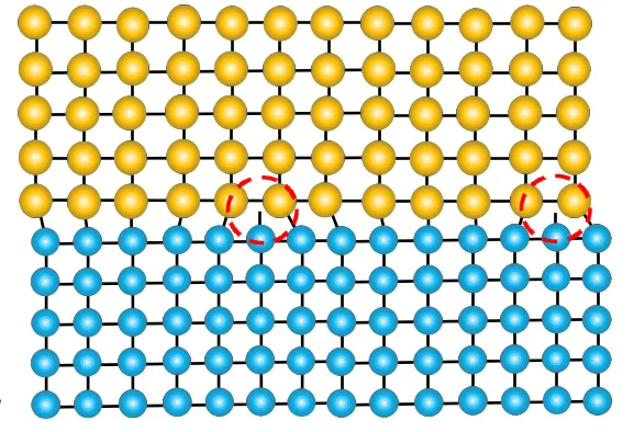 As shown above the lattice structure of Platinum too large compaired to Silicone meaning we would have addhesion issues if we tried to deposit directly on. To get around this we use the Titanium layer as a way to allow these two layers to stick together.
Setting up Sputtering
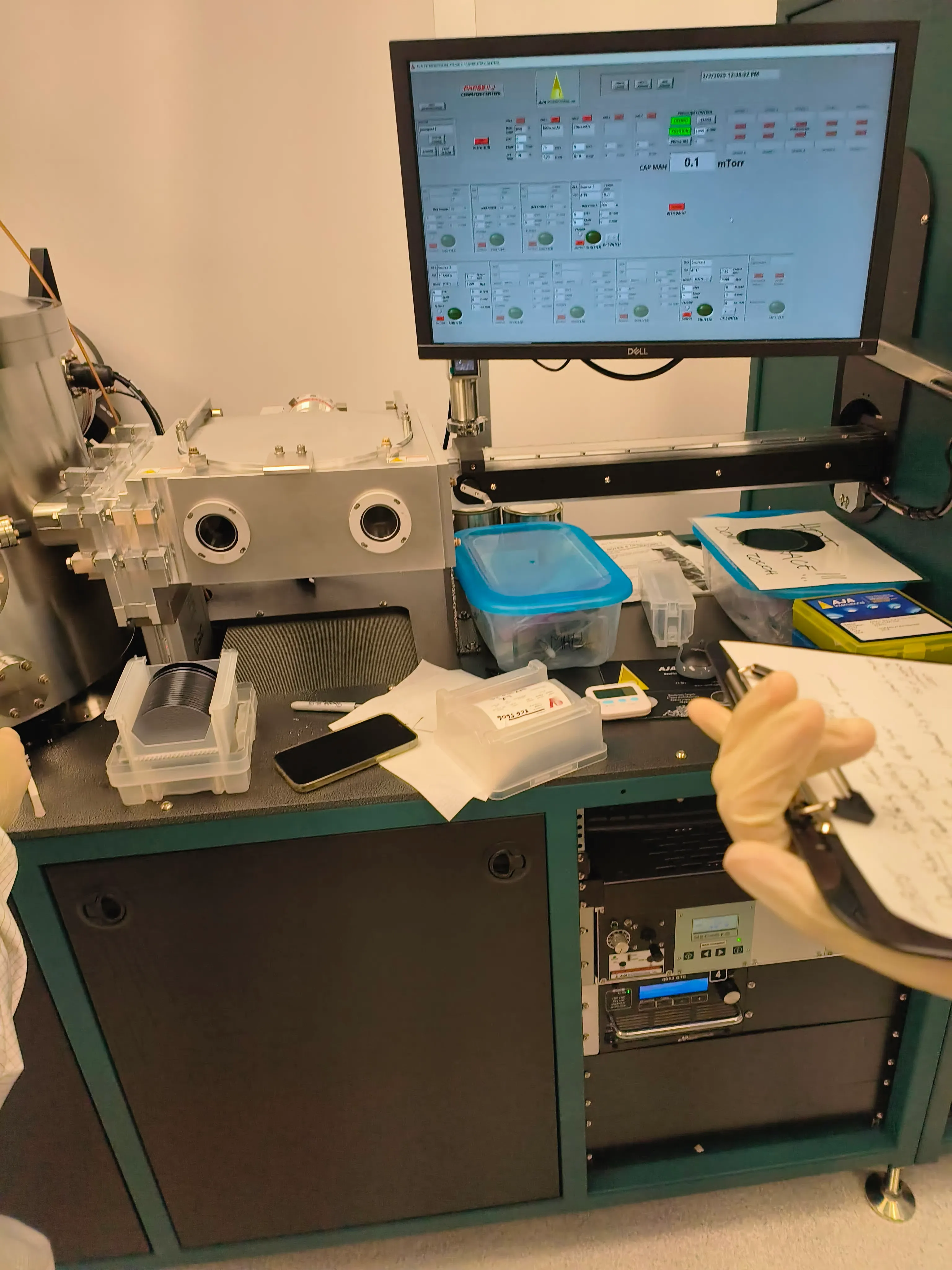
The process of Sputtering needs to be done in a VERY strong vaccume. We start the process at a pressure of 1.82E-7 Torr and we get the silicone wafer into the main chamber using a airlock chamber to avoid having to depressureise the entire chamber. Once we have the wafer in the chamber, we spin it for even coating. The Sputtering process works by using plasma to bombard a target which is a piece of the materal we want to deposit. This sends atoms of the target to the silicone wafer creating a layer. We use Argon as the gas of choise for sputtering and set the target to 200W, and run the sputtering process for 2 minuites. This will give us a thin layer of Titanum on our wafer of about 3-7nm which for reference is 1/15,000 the thickness of a human hair. 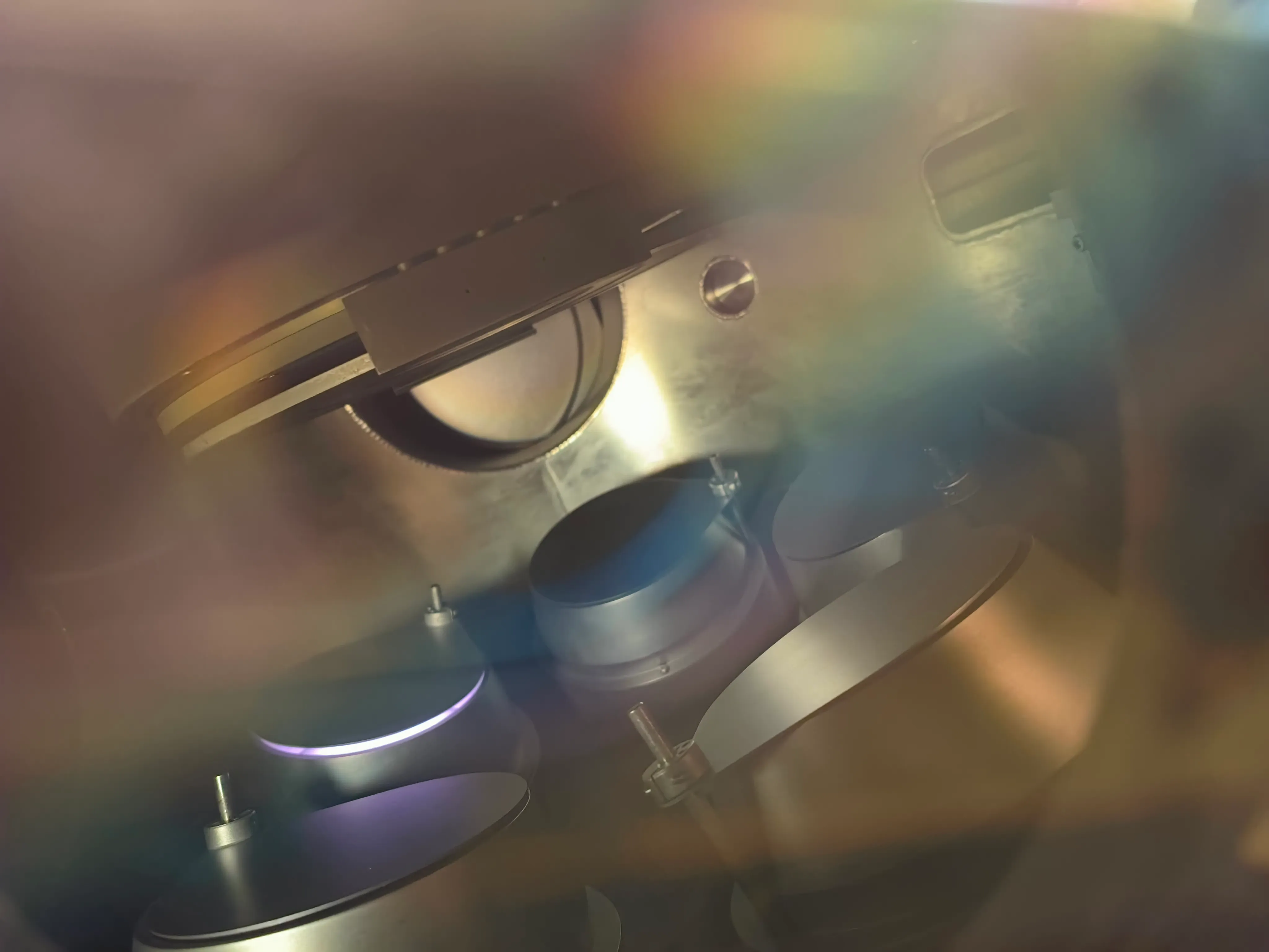 As shown in the image above, the purple/violet color is the plasma being formed. The metal covering it is called the shutter which we keep closed until we are ready to deposit. We do not deposit right away as we want to sputter off any oxidation which might have formed on the target before coating the silicone wafer. After we sputter on 3-7nm of we then are able to add a layer of platinum using the same method, however using a different target, one made of platinum instead. This time we set our target to 300 Watts and run the process for 15 minuites to get a thicker layer of Platinum. When forming the plasma, we need to slowly increase the wattage of the target at a rate of 1 Watt per second as to avoid thermal shock. As a target of platinum is basically just pure Platinum, we need to make sure it does not crack as that would be a very costly mistake. After 15 minuites we can slowly shut off the plasma and remove the wafer using the air lock chamber as before.
 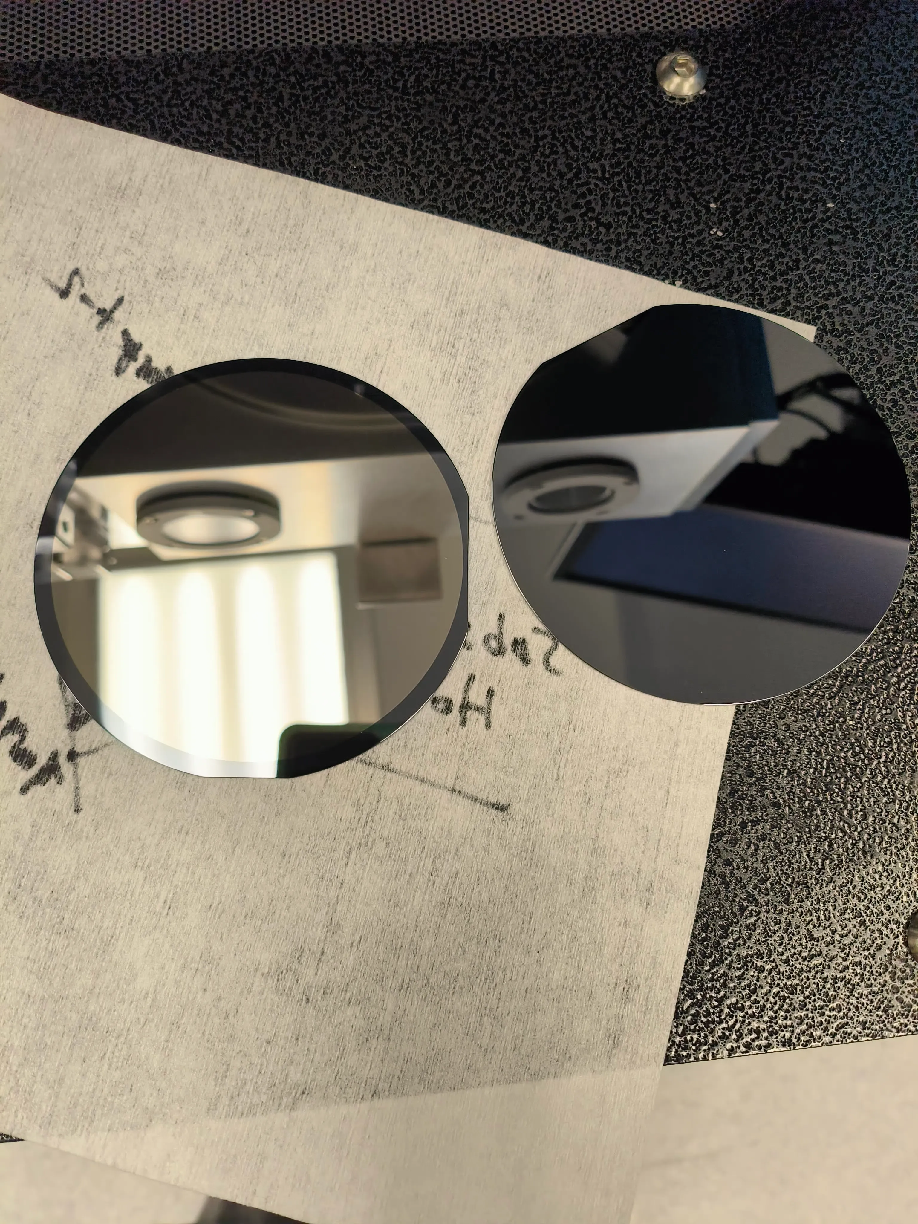 In the image above the wafer on the right is just a plain pure silicone wafer with crystal structure of <100> whereas the one on the left has a coating of pure platinum on it. It is perfectly smooth which is why is has a mirror finish which I think looks really cool.
ALD
Atomic Layer Deposition (ALD) is a chemical vapor deposition (CVD) method that deposits thin films of materal one atomic layer at a time. As you might guess, this process is much slower as it deposits a single attomic layer ever two cycles which takes around 2 minuites. While this process is much slower it makes the best conformallity resulting in near atomically perfect films. 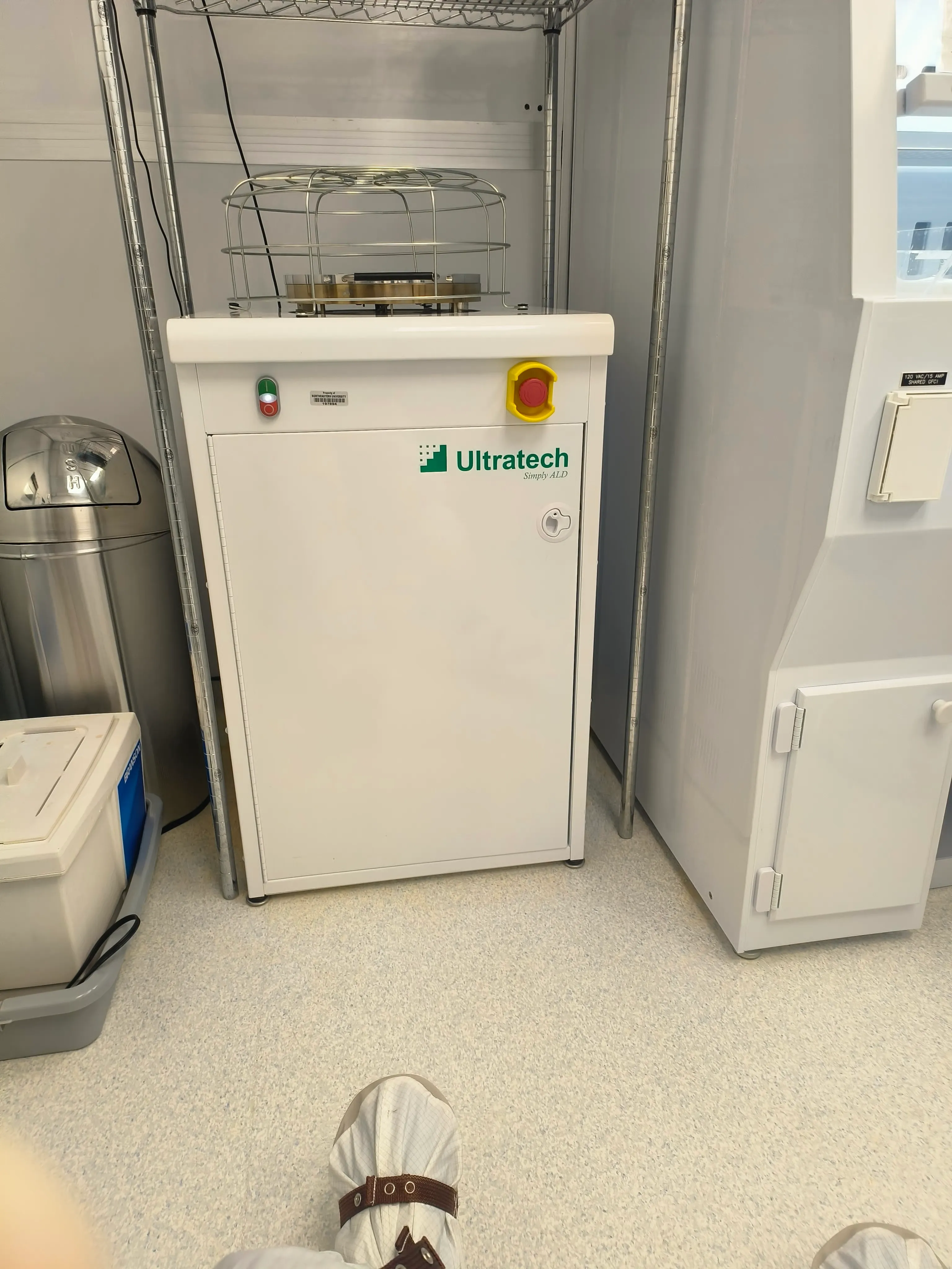 The ALD maschine is shown above, and is much smaller then the Sputtering maschine as it does not need to make any plasma, and only requires a vaccume level of 0.5 Torr which is a lot less strong.
 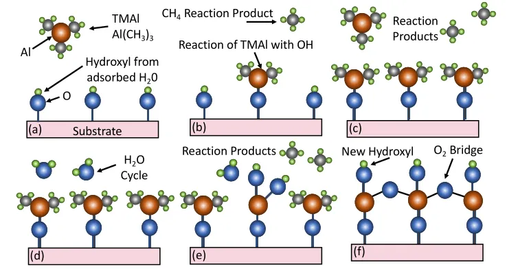 The process works as a chemical reaction in two different stages for a single atomic layer. It has a stage where it deposits a chemical which bonds to the substrate then flushes the system of water to finish the chemical reaction when the water oxygen atoms bond to the substrate and releases the excess hydrogen atoms as gas. For this process we did 104 cycles of Platinum followed by an additional 27 layers of Aluminum oxide which created a very thin film of 3nm. The overall rate of the ALD process is 0.5 Agnstrom per second compaired to the rate of 1 angstrom per second in sputtering. Despite being slower it is still used due to making near perfect layers, and avoids shadowing which is a side product of Sputtering or other PVD processes. Shadowing is when cavities or features on the silicone wafer are not evenly coated as it requires direct line of sight. Therefore for perfect application on steep walls or cavities, ALD is a must. Overall, I had a great time practicing these processes in the clean room.